5 February 2009
Cadence Tutorial 3: Cell Simulation and Characterization
Overview
The goal of this tutorial is to walk through the use of the transient
simulator which will be needed to characterize a cell's propagation
delays and effective resistance.
If you want to print out the tutorial just to have the steps
you can print the tutorial without screenshots
here. (It may be a bit out of date).
Alternately, if you print from Firefox, select print preview, and
scale it to 70% and then the screenshots fit nicely on the printout.
1. Setting up the Test Library
The first thing you need to do is create a schematic with the test
library and signal shaping inputs and outputs. For the tutorial and
the lab you will use the test libraries provided by Dr. Penry in
LabCharFiles.tgz from blackboard. Save this file in your library folder
in cadence and then "tar -xzvf template.tgz". You should now see two new
cells in your library manager "aoi21_1x" and "inv_1x". For our tutorial,
we are going to characterize a 1x inverter. You will shape the input
with two inverters and load the output with two inverters. Create a
new schemtatic "tutorial3" and insert instance with command "i" and
insert instances of inverters. Get the instance of inverter from your
library file. In our case you will add 5 inverters in a row (2 to shape
input, the test inverter and 2 to load the output). You will need vdd, gnd,
vpulse, and vdc from NCSU Anlog parts. Set the parameters of vpulse with "q" as follows
(you can also set parameters to show the values on the schematic. Don't forget
to set vdc to 5 volts as well):
Voltage 1 = 0V
Voltage 2 = 5V
Delay time = 0ns
Rise time = 100ps
Fall time = 100ps
Pulse width = 25ns
Period = 50ns
This will give you a nice symetric square wave input to the two shaping inverters.
Add some Vdds and Gnds and wire Vdd to the +5V of the constant source and Gnd to
0V of both voltage sources. You will need to connect the output of the load shaping
inverters to something (or Cadence will complain). A handy part is the "no connect"
found by doing "i" -> BYU_Basic -> noCon. To make identifying the signals
you are looking at easier, label the wire of the input and the output of the gate
in test: type "l", fill in the label name as "Input" then click on the wire for
the input and see the label appear. Do the same for the output. Save and check
the schematic. It should look something like the following:
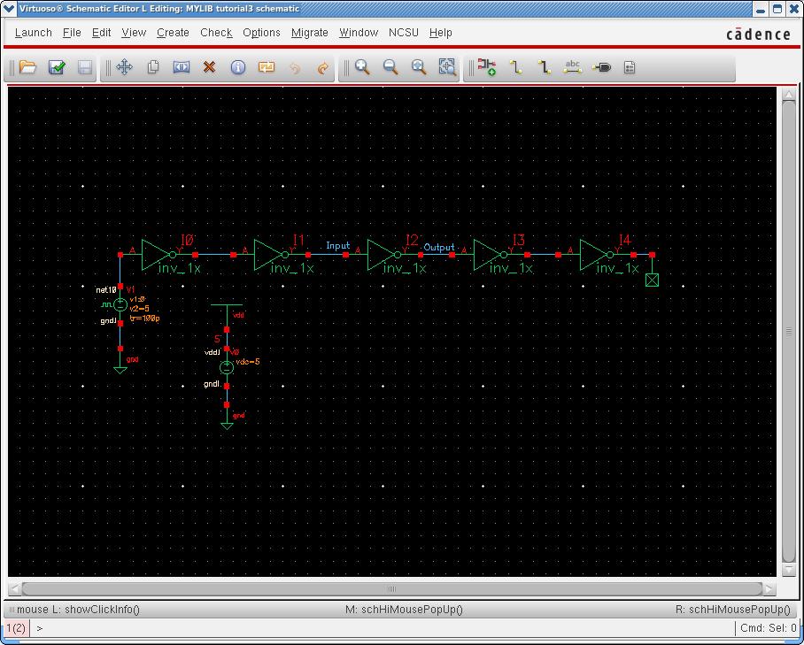
Screenshot 1 - Schematic
Note: In our case, since it is an inverter we have already connected all of our
inputs. When characterizing a gate that has more than one input, each unused input needs
to be tied to vdd or ground. You need to plan your simulation so that you hold imputs
so that the output toggles high or low with the input changing. Note that we are using
analog extracted views (they are already all included in the tgz file provided.)
2. Creatig a config view
2.1. In the Library manager window: File -> New -> Cell View...
2.2. in "view name" type config (The "Tool" field should automatically change to Hierarchy Editor).
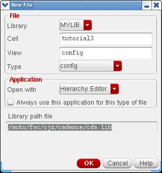
Screenshot 2 - create new file
2.3. Press OK. A couple of windows will pop up. "New Configuration" will be on top. Click on "Use Template"
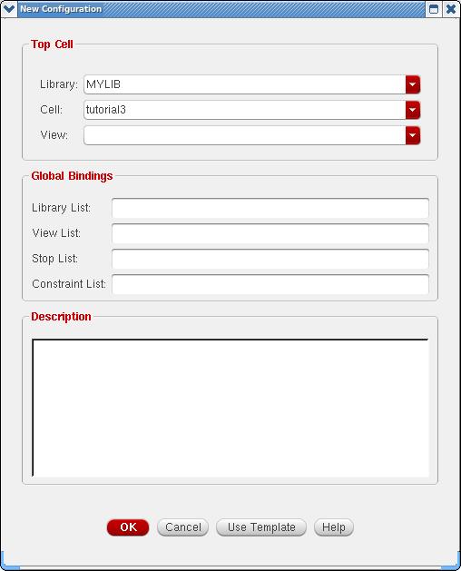
Screenshot 3 New configuration
2.4. In the "Name" field choose "spectre" in the dropdown list.
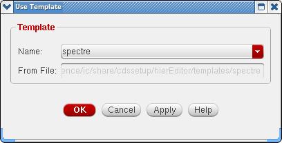
Screenshot 4 Choose Template
2.5. Click OK.
2.6. In the "View" field of the New Configuration window, change from "myView" to "schematic"
(drop down). When complete it should look like the screenshot below.
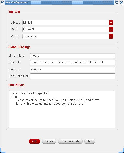
Screenshot 5 filled in new configuration
2.7. Click OK. You will now be in the hierarchy editor.
2.8. Right click on inv_1x
Set Cell View -> analog_extracted.
NOTE: in the actual lab you will be simiulating both and inverter AND AOI21.
You need to do the same operation on the inv_1x AND the AOI21_1x.
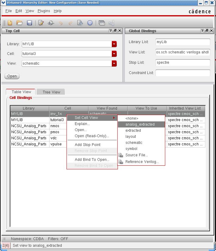
Screenshot 6 screenshot with the right click showing
2.9. Click the disk (save) icon
2.10. Click upper right hand corner to close the window.
You should now be looking at your schematic. (Open your schematic if it is not open).
3. Setting up the Analog Design Environment
3.1. On the Schematic menu launch the analog design environment by clicking Launch -> ADE L
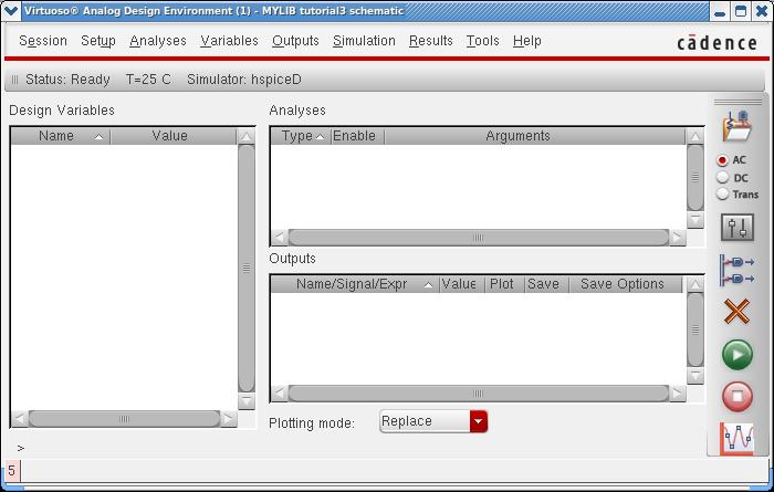
Screenshot 7 Analog Design Environment
3.2. Setup -> Design
3.3. Select tutorial3 (select the name of the schematic you created), change view name to
"config". Leave Open Mode as "edit".
NOTE: the screenshot erroneously leaves the view name as schematic.
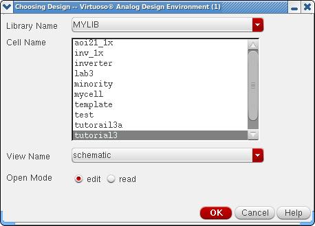
Screenshot 8 Choosing Design
3.4. Click OK. A second ADE window will open. Close this extra window.
3.5. Click Setup -> Simulator/Directory/Host...
3.6. Select Simulator "spectre" from the drop down list. (Leave the other options alone.)
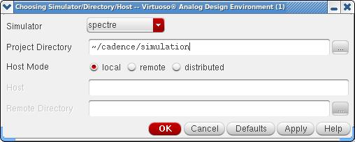
Screenshot 9 Selecting Simulator
3.7. Click OK.Again, a second ADE window will open. Close this extra window (leaving the one that says "Simulator: spectre" in the status line under the menu bar.)
3.8. Select the model library. Click Setup -> Model Libraries...
3.9. Click on the "..." on the right
3.10. I found the easiest way (there are other ways, including typing ahead) to get the path
filled in is to navigate up to top
(by clicking on the up arrow folder icon 4 times) and then double click on the "opt"
and then the "Cadence" folder etc. Ultimately the path needs to be fille din with
/ee2/Cadence/local/designkits/BYU/lib/AMI12/models/spectre/allModels.scs
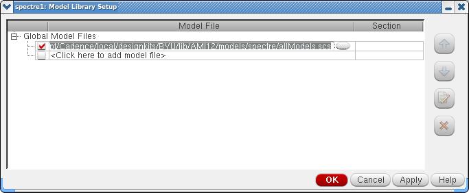
Screenshot 10 Model library Setup
3.11. Click OK. Your analog Design Environment should look like the below.
Screenshot 10a - Filled in Analog Design Environment.
4. Running a Simulation
4.1. Set up the length of our transient analysis: Analyses -> Choose...
The "tran" radio button will already be filled in. You will want to run the analysis
at least two periods. In our case we will fill in 150n (which is 3 periods). Click
moderate and (and at the same time the enabled checkbox will be filled)
Note: if you don't get the dialog in the picture below, then check your
simulation setup from the last section.
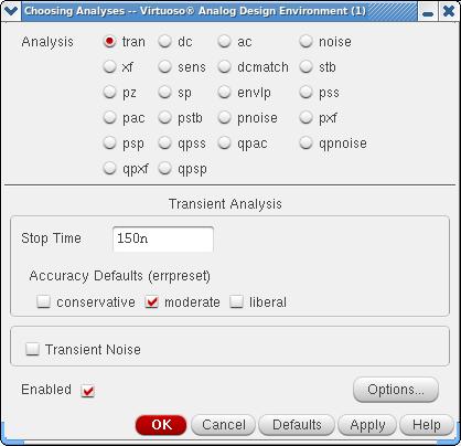
Screenshot 11 choosing analyses
4.2. Next we want to choose the outputs to plot:
Outputs -> To Be Plotted -> Select on Schematic
The Schematic will come up. Click on the wire for your input and the wire for your output.
The wires should highlight in a dotted line. If you get a circle around a node, you clicked a node
(nodes measure current, wires measure voltage.)
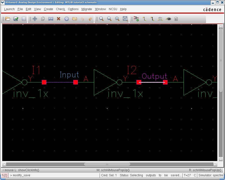
screenshot 12 Schematic
4.3. After you have selected the input and output, hit esc.
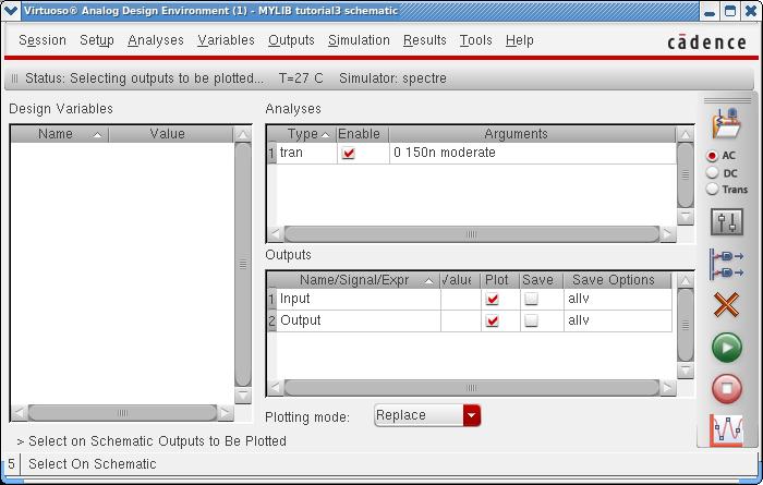
Screenshot 13 Analog design environment filled in.
4.4. click the green button to run the simulation
4.5. A graph will appear
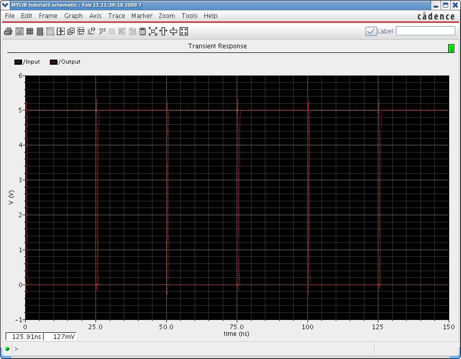
Screenshot 14 the graph
4.6. You will want to switch to strip mode (so you can see the input and output separately).
Click on the 4th button from the left. On the right hand side of the graph you can change the colors
so things are easier to see. There are lots of things you can do - you can zoom in,
you can turn the grids off, etc. You can place the mouse over the wave form to have it display the values
in the lower left hand corner. By going to 2.5 v and recording the time when the input rises and then
recording the time when the wave falls on the output, you could get the delay right from the graph.
In our case you could record 340ps on the rise and 500ps on the fall for a propagation delay of 190ps.
In the next section we will use a calculator to get readings.
UDATE: Note The numbers here are WRONG. You should see a delay of about 215 ps! (If you get 190 then you
didn't use the config view in the choose design step above.)
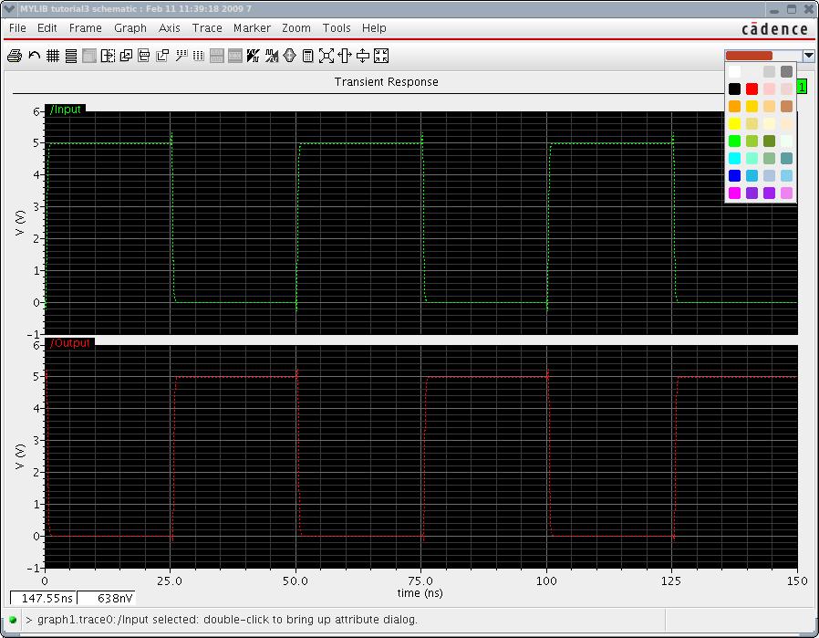
Screenshot 15 Graph (circle the strip mode and the change colors)
You can zoom in on the graph as follows: a) click on the zoom button b) click and hold on the left of the
graph c) drag the mouse just to the right of the first rise in the input. d) release mouse button. e) repeat
to zoom in further. You can really stretch out the graph and make measurements right on the graph. In the next
section we will use the calculator to take measurements.
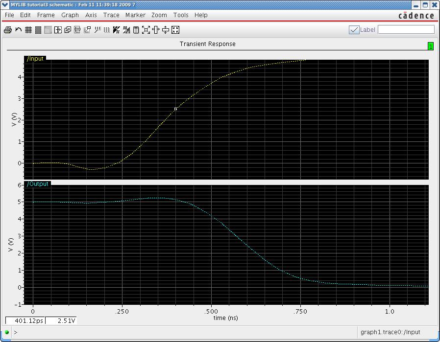
Screenshot 15a zoomed in
5. Using the Calculator
5.1. On the graph there is a calculator icon or you can start it from the tools menu
(Either from the graph or from the Analog Environment window). Start the calculator.
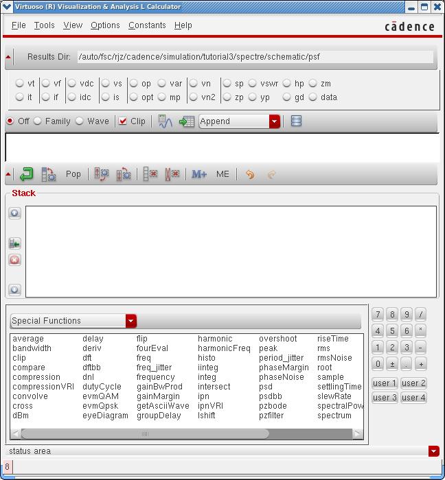
Screenshot 16 - Visualization & Analysis Calculator.
The calculator has many, many functions and the online help is well written. As a quick overview,
The calculator uses reverse polish notation and has a current buffer and stack. It has the capability
to read the graph and trigger on rise and fall. We will use the calculator to do a propagation delay
that we read from the graph in the last section.
5.2. In the special functions section at the bottom, select "delay" We will fill in the parameters for this
function to allow the calculator to find the delay.
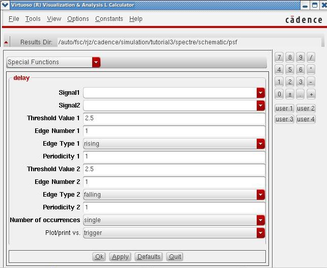
Screenshot 17 Special functions section
5.3. We will get the voltage wave form right from the schematic: click on the radio button "vt". You will be switched to
The circuit. click on the input wire.
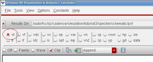
Screenshot 18 - vt radio button
5.4. Switch back to the calculator and notice the VT("/INPUT") on the buffer.
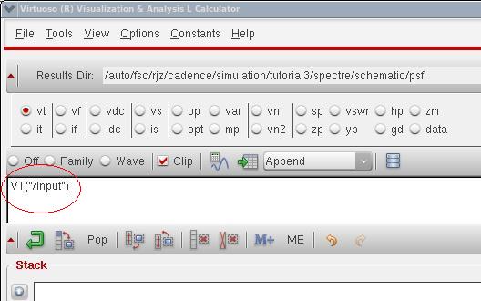
Screenshot 19 - buffer
5.5. In the special function "Signal1" dropdown, select "buffer" and notice that the information from the buffer is copied
into the field.
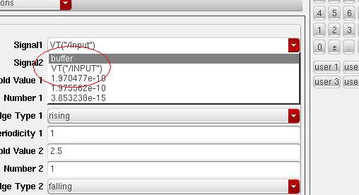
Screenshot 20 - Signal1 dropdown
5.6. Click on the button to clear the buffer
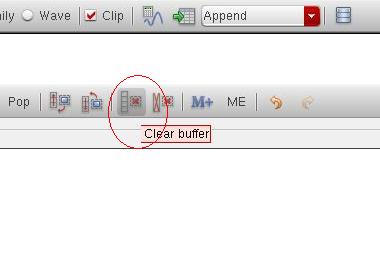
Screenshot 21 - Clear buffer button
5.7. Go to the schematic and select the output and repeat steps 4-6 for Signal2.
5.8. Fill in the remaining values as follows:
Threshold Value 1: 2.5
Edge Number 1: 1
Edge Type: rising
Periodicity: 1
Threshold Value 2: 2.5
Edge Number 2: 1
Edge Type: Falling
Number of Occurances: single
Plot/print vs. :trigger
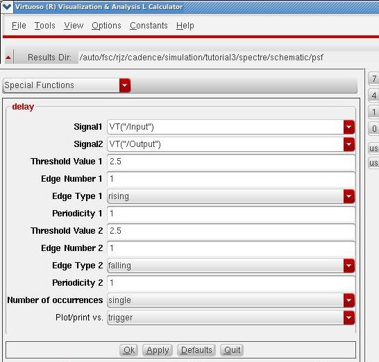
Screenshot 22 - input values
5.9. Click OK and the function is placed in the buffer
Screenshot 23 - function filled in the buffer
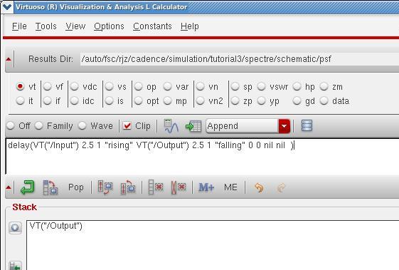
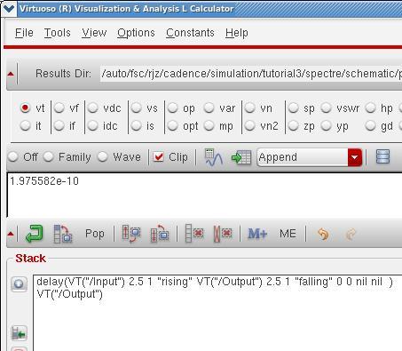
5.10. Click the Evaluate button. The result (1.975582e-10) is placed in the buffer
(the equation is now on the stack). This is pretty close to the 190ps we figured in the
last section.
UPDATE: The numbers in the tutorial are WRONG. You should be getting something like 215ps.
Screenshot 24 - The calculator output
NOTE: In this tutorial we found tpdf (time propagation delay fall). If we wanted the rise we
would have had to use falling edge input and rising edge output.