Introduction
This tutorial takes you through the IC Craftsman Chip Assembly Router. The router is yet another tool integrated into the cadence environment. Unlike the schematic and layout virtuoso tools, which are part of the integrated circuit (IC) toolset, this tool is part of the IC Craftsman (ICC) toolset. The reason you need to know this is so when you are looking for documentation on the tool you look in the correct documentaion location $CADENCE/icc/doc.
This router is best at routing together large functional blocks, such as serveral PLAs comprising a project. It is not very good at routing data path intensive units, but luckily for us most of the datapath intensive routing is already done inside the PLAs.
The tutorial will teach you how to set up your schematics and layouts to use the router, how to export your design to the router, how to run the router and then how to import your design back into Virtuoso layout. During this explanation, the tutorial walks you through each of these steps for an extremely simple counter realized in a PLA.
| Introduction |
| Preparing Schematics and Layout |
| Using the Router |
| Conclusion |
| plagen |
| ctr.pla |
| ctr.ctl |
| ami12.rul |
| ami12.do |
Preparing Schematics and Layouts
When using the chip assembly router, start with a schematic that has already been simulated and verified using the verilog-xl simulator. Every instance used in the schematic must also have a layout view that succesffully passes LVS. If for some reason one of the instances does not have a layout you must go back and fix it before continuing.
The router only understands 'shape' pins. If you have followed all the tutorials to this point, you should have no problem with this. If you haven't then you need to go verify that all your pins were made using either metal1 or metal2 drawing (dg) layers, not pin (pn) layers. The PLA generator used to create PLAs with the incorrect layer for its pins. It is now updated to use drawing layers. If all your PLAs still have pin layer pins then get the new plagen and re-generate all your PLAs.
Ok, let's set up the test PLA. Download the PLA counter files:
Run plagen on the file. You should have three files, ctr_s.il, ctr_l.il and ctr.v. Load these into cadence following the same procedure you learned in the PLA generator tutorial. Make sure you follow all the steps, including creating the functional cellview.
Do the following for the counter fixing any problems that arise:
- Check and save the schematic. You will most likely have some floating net warnings, ignore these.
- Run DRC on the layout. It should pass with no errors.
- Run Extract on the layout to create an extracted cellview.
- Open the extracted cellview and LVS it with the schematic. LVS should succeed and the net-lists should match.
- Click the Build Analog button in the LVS dialog box to create an analog-extracted cellview.
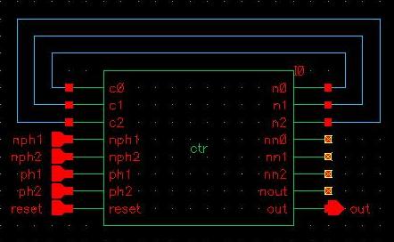
The next step is to go to your test library and create a new schematic called pla_test. Instance the counter, connect all the state feedback lines and create inputs on the reset line and all the clock lines. Also, create an output on the out line. Your schematic should look like the figure.

Check and save the schematic.
Next, go to Tools->Design Synthesis->Layout XL. This will open a couple dialog boxes prompting you to create a new layout cellview from the current schematic. Agree to their demands. Cadence will open a layout window next to your schematic window.
The new layout does not have anything in it yet. Instead of instancing each component by hand, have cadence instance everything for you. Select Design->Gen From Source in the layout menu. You will see a window looking like the picture below. Make sure your default pin layer is metal2 and that your pin type is geometric. Click update so that all the pins are metal2. Now, using the update button below the pin assignments, change all your input and output pins to metal1. Leave the clock phases, as well as power and ground, as metal2. Click OK. (Do not worry if vdd! and gnd! do not show up in the list. The generator creates them using the default metal.)


Your instances are at the bottom of the laout. When you have more of them you will notice that they appear in roughly the same arrangement you used in the schematic.
Back to the layout. Click on the layout and select the move tool. Select the counter block and drag it up into the boundary area. When you start moving the block you will see a lot of little lines appear. They seem to be pointing towards the origin. The are actually showing you where the nets you need to route are. After dragging the counter block into the boundary area, zoom in on the origin. You will see little squares of metal1 and metal2 labeled with all your pin names. You will place these where you want the external contacts located.
Select the move tool and get the counter lined up exactly with the origin. Use the stretch tool to shrink the boundary layer down so that it is exactly the same size as the PLA. If you cannot select the boundary, go to the LSW, choose edit, find prboundry and click on the dg box so that it is a valid layer.
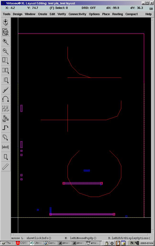
Place all the pin contacts on top of their respective nets. In order to do this open the display editor, set the display level to 2 or deeper and click on show pin names. The clock phase pins and the input and output pins are already the right size so just place them right on top of their respective nets. Stretch the power and ground pins so that they cover the PLA pins. Your layout, with the display level set back to 0, should look like the next figure.

Now, and this is extremely important, run DRC. You should pass with no errors. You should always run DRC before sending a layout to the router.
Some of you may get a DRC error stating that a label is invalid because it is on a net with a different name. If this happens, take your reset pin and move it down 1.8u. For some reason, the ground bus on top of the reset pin in the PLA tries to pick up the pin label. I don't know why, but you can fix it by moving the pin down a little bit.
At this point you are ready to route.
Using the Router
The chip assembly router cannot do its job unless you tell it the design rules. Luckily for you I have already packaged up the rules in the format the router expects. You tell the router the rules using two text files
The first file, ami12.rul, is passed to the router when you start it. The second is run first thing after the router starts. On to routing the counter.
Once you have a layout that passes DRC you are ready to send it to the router. Select Routing->Export to Router from the layout menu. You will see a dialog box looking like the following figure. The defaults are mostly OK, just change two things. First, click the Use Rules File button and browse to the location you left the ami12.rul file. Second, select Cadence Chip Assembly Router. Click OK to start the router.


Follow the next few steps to route your design:
- Goto File->Execute Do File and run the ami12.do file you downloaded earlier.
- Goto Autoroute->Global Route->Local Layer Direction and choose Layer Panel on the dialog box that appears. Click OK to close the window.
- Goto Autoroute->Global Route->Global Router and say OK in the dialog box that appears.
- Goto Autoroute->Detail Route->Detail Router and say OK in the dialog box that appears.
- Your design is now routed. It may have some errors. Don't panic. We still have some post routing operations to perform and some of the do a good job at removing these little errors.
- Goto Autoroute->Clean.
- Goto Autoroute->Post Route->Remove Notches
You should now have a nicely routed design. Save it by selecting File->Write->Session. Go back to the layout window. Sometimes the routed design is automatically imported back into Virtuosos Layout. If it didn't appear, go to Routing->Import From Router and read in the session you just saved. You should see something like the figure below.

Conclusion
The router has a lot of options you can set, including costs for routing vertically with metal2 and horizontally withe metal1 (usually these are taboo.) Feel free to poke around inside the router in order to make it work better for you. All we ask is that you document what you've done and explain it briefly in your writeups. That way we can continue to improve the cadence knowlege base.