An extremely powerful concept in VLSI is the standard cell library. Standard cells help create efficient dense layouts because they are easily abutted during the layout process. Standard cell layout simply means that all standard cells - nand, nor, not, etc. - in the design are layed out with standard dimensions for heights, widths, actives and wells, and have standard power (vdd!) and ground (gnd!) busses. This tutorial discusses standard cell design for the AMI12 library.
Sections 1, 3, and 4 discuss the steps executed while creating a standard cell library. Sections 2 and 5 contain an example inverter created following the instructions in sections 1, 3 and 4.
It is much easier to ensure that your standard cell library is actually standard by creating a standard cell template which you copy into your individual cell layouts. All the standard cells in your library will have a fixed height. We're going to set it at 27 lambda. They will all have a minimum width, but can be wider depending on the size of a cell. For instance, inverters are very narrow, nand gates are somewhat wider, and flip-flops are much wider. When you need wider cells, simply abut two standard cell templates together.
Allright, you need a library to place your standard cells in. Fire up cadence and create a new library called stdCellLib. Attatch it to the AMI12 technology library. Create a new cell in the library. Name it template and select layout.
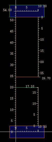
Use the ruler to measure out an area 54 u tall and 10.2 u wide. Use the 0,0 origin as your starting reference point. Your layout view should look like the picture.

Make a power bus at the top of the cell. Use metal1 to draw a rectangle 4.8 u by 15 u. Notice how it hangs over the edges of the area we defined with the ruler? This is so the cells adjoin easily later on. It should hang 2.4 u over the edge.

Copy the metal one rectangle and place the copy at the bottom of the cell. This is your ground bus. Make sure it also hangs over the cell area you defined the same way the power bus does.

Because the vdd and gnd busses will be embedded in nwells and pwells, we need to put nselect and pselect around them. Put an nselect region around the vdd bus. Make it 0.3 u larger on every side than the metal1 rectangle. Put a similar pselect region around the gnd bus.

Generally the pullup devices are larger than their corresponding pulldown devices. Planning for this, draw your n-select and p-select regions. Make the pselect region take up about 2/3 of the cell. Draw a pselect rectangle 26.7 u high by 10.2 u wide. Butt it up against the nselect around the vdd bus. Draw an nselect rectangle 17.1 u by 10.2 u. Butt it up against the pselect around the gnd bus. Note, it will help you to watch the delta X and delta Y coordinates at the top of your screen while drawing rectangles.

Create the pwell and the nwell. The nwell goes around the p-type transistors and the pwell goes around the n-type transistors. The wells should extend 0.3 u around the p and n select boxes surrounding the vdd and gnd busses. They should meet exactly between the p and n select boxes in the body of the cell.

Create contacts to connect the vdd and gnd busses. This helps avert latchup. To create contacts press 'o' and select M1 to Active. Place three contacts on the vdd bus and three on the gnd bus. Make sure they are placed exactly at (0, 0), (5.1, 0), (10.2, 0), (0, 54), (5.1, 54) and (10.2, 54).

In order to see what is inside the contacts, press 'e' to bring up the display and set the display level to 10.

Run DRC to make sure your standard cell contains no errors and save it.
Lets use the standard cell template created in the previous section to add an inverter to the standard cell library.
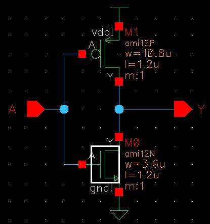
The first step is to create a schematic of the inverter. Open up your standard cell library and add a new cellview. Call it inv and choose schematic for the cell type. Draw the schematic shown in the figure below paying special attention to the transistor widths and model names (setting the model name is explained below).

Note: in order to set the model type correctly, you need to open the properties window, set the model type to user and the model name to ami12N or ami12P depending on which transistor you are using. Generally you wouldn't have to do this step because the library designer would have automatically linked the transistors to the technology file. Unfortunately, our technology file is not configured completely, so we need to do this manually. Whenever you place a transistor while using the AMI12 tech file you must change its model name to ami12x.

Check and save the schematic. Choose Design -> Create Cellview -> From Cellview and make a symbol for the inverter. It should look something like the picture below. Note, in order for me to get my circle sized correctly I opened the design options 'e' and changed snap to grid from 0.0625 to 0.03125.

Go ahead and save and close the inverter schematic and symbol.
Create a new cellview called inv but this time choose layout for the cell type. Also open up the standard cell template layout. Select the entire template, press 'c' to open the copy dialog, click somewhere in the template and them move the mouse over to the inverter layout window. Place the template in the inverter layout. Carefully place the lower left contact right on the origin. Remember, in order for the standard cells to abut correctly they need to share a common origin.
Odds are the contacts do not look right. Press 'e' to open the display options and set Display Level Stop to 2.
Draw the inverter making sure it matches the pictures below and that the transistor widths are correct.
The inverter pullup: Draw a box of active 7.8 u by 10.8 u. Place a bar of poly 1.2 u wide. It should overlap the active by 1.2 u. Press 'o' to open the contacts menu. Select metal1 to active contacts, 1 column, 4 rows and place them as shown. Make a small rectangle of metal1 to connect the left side contacts to the vdd bus. Note: running DRC at this point is a good idea. It should pass easily. If it doesn't, make sure all the layers are sized correctly and try again.

The inverter pulldown: Draw a box of active 7.8 u by 3.6 u. Stretch the bar of poly from the pullup section down to the pulldown section. Make sure it overlaps the active by 1.2 u. Press 'o' to open the contacts menu. Select metal1 to active contact, 1 column, 1 rows and place two of them as shown. Make a small rectangle of metal1 to connect the left side contacts to the gnd bus. Note: The layout should pass DRC at this point.

The contacts: Placing contacts in standard cells is easy. The only things you need to think about are routing lanes. You want to be able to route horizontal tracks of metal 2 over your standard cells. Parallel metal 2 paths must be separated by 2.4 u. That means you can theoretically have a metal 2 path every 4.2 u - that is, 2.4 u between paths and the paths are 1.8 u wide. Our cells have routing tracks every 6 u. This gives us a little extra room to manuver if we need it.
Start on the x-axis and draw a ruler up the right hand side of the inverter. See the figure below. Place your output contact at 27 u or 21 u. Place your input contact at 15 u. The input and output contacts are metal 1 to metal 2 vias. In order to hook the input contact up the the poly, place a metal 1 to poly contact next to the poly, connect it with a small piece of poly and then connect it to the input contact with metal 1. The reason we didn't just stack this up is that the process doesn't allow stacked vias. Most newer processes do, this is just a quirk of the technology we are working with.
Your contacts should look like the figure below.

Naming pins: Place two metal 2 layer shape pins and two metal 2 layer shape pins. First, select metal 2 in the LSW. (LSW stands for layer select window, it is probably on the left side of the screen.) Go to Create -> Pins and open the create pins window. Select mode as shape pin and make sure rectangle is selected. Select Display Name. In the terminal names block, type A Y. Select I/O type as input. The create pin box should look like the figure.

Go to the layout and draw a rectangle directly over the metal 1 to metal 2 via on the input. Change I/O type to output and do the same for the output via. You should see something like the figure.

Now select metal 1 in the LSW. Create vdd and gnd shape pins on top of the gnd and vdd busses. Set the I/O type to inputoutput. Your finished inverter should look like the figure.

Now make sure the inverter is correct. Run DRC, extract the inverter and run LVS. After a seeing net-lists match, press the Build Analog button in the LVS window.
Characterizing a cell involves simulating a bunch of situations the cell could find itself in and writing down the results in a format other cadence tools can use to further the design. Open this pdf document to learn how this is done. (When I get a chance I'll make this part of the html as well.)
Charcterizing Cells - Technology Library File
The document references a text library file called sample.lib.