
Getting familiar with Virtuoso Schematic


The "Create New File" window will open and you will be prompted to choose the cell view and name the cell. Since you are building an inverter, enter the name "inverter" in the Cell Name field and verify that "schematic" is written in the View Name field. The Tool should be "Composer-Schematic".

Descriptions and corresponding hot keys are given below for each of the icons in the toolbar. One important function that is not listed is using the "ESC" key. Whenever you are finished doing something, such as placing a wire or an instance, it is a good idea to hit "ESC" to escape that function. That way, when you want to move on to the next function, you will not still be stuck in the previous function.

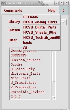
In order to build an inverter, you will need a N-MOSFET and a P-MOSFET. These can be found in "NCSU_Analog_Parts" library. To place a component, click in the instance icon or type 'i'.
First, you must select the library where the parts are located. Select the "NCSU_Analog_Parts" library to find the N-MOSFET and P-MOSFET.
The list now displays all of the categories of components in the library selected. Each of the components can be found in their respective category. Since you want to select a N-MOSFET, select the "N_Transistors" category.


 Select the "nmos" component and the parameters for a NMOS are displayed in the add instance window on the right. The parameters can either be edited now or later, using the property function. For now, just place the part. You can edit it later.
After selecting "nmos", simply move the cursor into the Virtuoso Schematic Editing window and the cursor will turn into the component you are trying to place. In this case, place the nmos somewhere in the middle of the schematic. If you are unhappy with where you placed the nmos, you can use the move function (hotkey - m) to move it later.
Follow the same procedure for a P-MOSFET, which can be found in the "P_Transistors" category, under "pmos". Place the pmos above the nmos in the schematic. In other schematic designs, it is common to use the 4-terminal bulk MOSFET devices. If you were to use these in this simulation, you would need to select nmos4 and pmos4 (found in the same library) instead of nmos and pmos, respectively.
Also, under the "Supply_Nets" category, place the vdd component above the pmos and the gnd component below the nmos. The vdd and gnd symbols are global. In other words, if you were to connect a node to another vdd symbol, then that node would be connected to anything else that is connected to a vdd symbol. So later, we can actually define what vdd is (a voltage) by connected it to a voltage source. For example, if we connect vdd to a 5 V constant, DC source, then the any node that is connected to a vdd symbol will be also connected to the 5 V source. The gnd symbol is a reference (or common) node used in simulation. Since you are done placing the necessary components, hit 'ESC' to exit the component placement function. After placing the four components, your schematic should look like the picture below.

Notice that the parameters of the transistors appear next to the transistors. These parameters are among the many that can be changed to model the transistor to the designer's desire. To change the parameters, click the property icon, or hit "q". Then, click on the component that has parameters that you want to change.

The "Edit Object Properties" window appears. If the box is too small, scroll down to view all of the parameters or enlarge the window. When changing parameters of the nmos or pmos, you will most likely be changing the width and length. Notice the parameters Width (minimum) and Length (minimum). These parameters are shaded in. This is because these are the minimum values and in the Width and Length parameters, you cannot enter values that are less than the minimum.
Since in most inverters, the width of the pmos is usually made to be 2-3 times larger than the width of the nmos, make the width of the nmos 3u and the width of the pmos 6u. The proper notation includes the value, a space, and then the units. So if you wanted to enter .0045 millimeters, you would enter .0045 M or 4.5m M. You normally do not need to type the units because it will be entered by default. Do not change any of the other parameters. After changing the parameters, hit 'ESC' to exit the edit properties function.
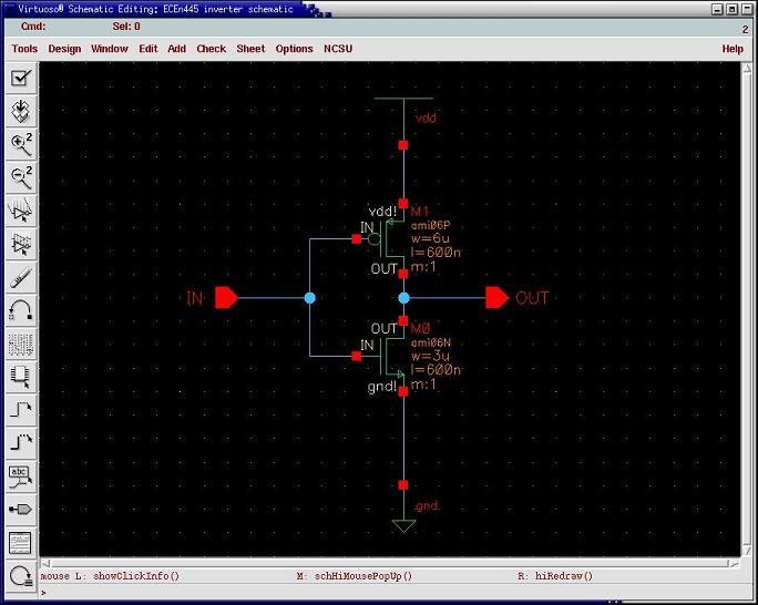
Next, the components need to be connected to eachother using wires. This can be achieved by using the Wire (narrow) icon or by typing 'w'. The Wire (wide) icon or 'W' is for busses. Connect the following using the narrow wire:

The final schematic should look something like the picture below.

The next step is to select the "Check and Save" icon or type F8 and make sure there are no errors. If there are any errors or warnings, a window will appear, otherwise everything should be okay. You can verify this by looking in the log, listed in the Command Interpreter Window.
Now that you have drawn up your schematic, you will need to create a symbol for it. Then, if you want to use the inverter in other schematics, you can place the new symbol that you will have created.

First, select Design-> Create Cellview -> From Cellview...

As long as the From View Name field reads "schematic" and the To View Name field reads "symbol", then nothing needs to be changed, and you may select OK.
Virtuoso Symbol creates your inverter, but you should make some changes to make it look like an inverter. The red lines make up the outline of the symbol. This outline should border all of the outer dimensions of the symbol. It will be invisible when placing the symbol. The green lines make up the actual shape of the symbol. Like the red lines, these lines can be moved, added or deleted, or stretched. These lines will appear when placing the symbol in a schematic. The green "[@partName]" text can be edited (using the property icon or 'q') to name the symbol and the red "[@instanceName]" text should be moved closest to the symbol. This field will designate the component among others. For example, if you had two resistors, one would be R0 and the other R1. Therefore, it is important to have this field close to the symbol. Remember to hit 'ESC' each time after using a specific function.

Use the line icon to add lines to the symbol. When selecting this icon, the Add Symbol Shape window will appear.

Several different shapes can be added, such as circles or rectangles by selecting the various shape options in the Add Symbol Shape window. Since we are making an inverter, the symbol should look like a triangle with a small circle at the tip of one of its corners. A good way to begin would be by deleting the green box. Then construct (using the line function) a triangle within the red box. Before making the triangle a little larger though, extend the red box borders by using the stretch command (type 's').

Next, using the Add Symbol Shape window, draw a circle at the tip of the triangle. The first place you click will act as the center of the circle you are drawing. As you bring the cursor away from that point, the circle's size will change. Move the labels and lines around that everything is not too cramped together. Make sure that the pins are located on the red box outline. You do not want the symbol to take up more space then is necessary.

Save your symbol (F2) before proceeding to the next tutorial, Simulating an Inverter.